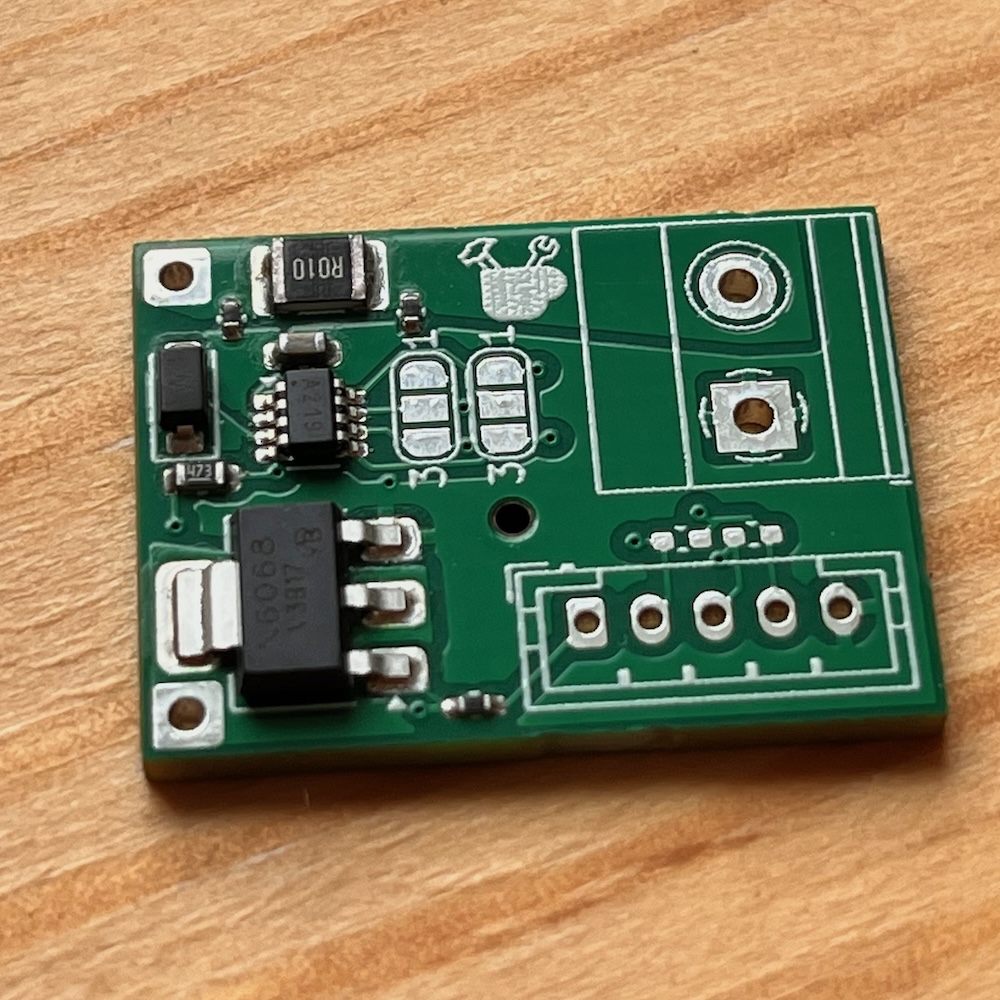
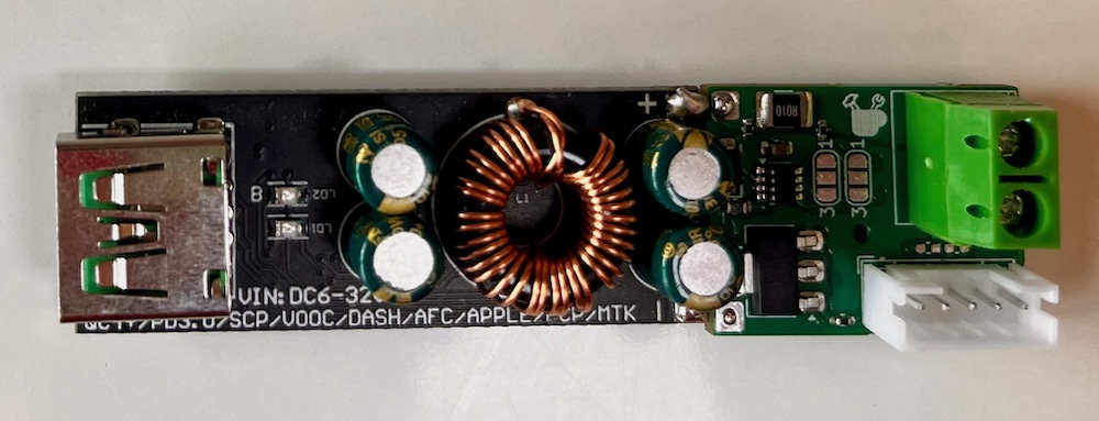
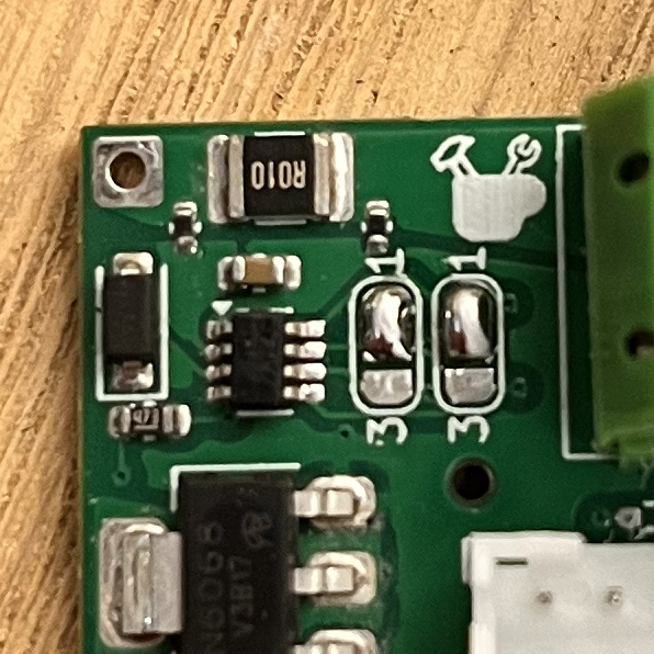
Quick recap of my USB-C PSU build: I have these USB-C supply boards from aliexpress that take 24v and supply up to 100W using the standard USB-C PD profiles. I designed this little board to add enable/disable with a mosfet and power monitoring with an INA219. In the end, many of these boards will go into a lasercut case with a Meanwell 240W 24V PSU and a microcontroller to turn some of them off if the combined draw gets too high.

I’ve had these boards back from the board house for multiple months and have only just gotten around to testing them. Here’s the sequence of tests I went through, trying to rule out basic errors before moving onto things that might kill it.
- Supply 3V through a lab psu with a variable supply. Initially with a very low current limit, ramp the current limit to check for dead shorts.
-
Connect up I2C and see if the INA219 responds.
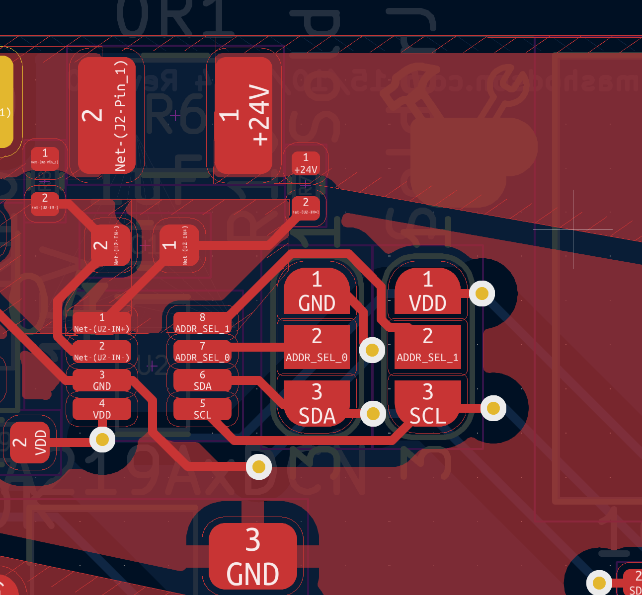
- Find the INA219 on I2C at address 64 (0b1000000) which makes sense assuming the floating address pins have a pulldown resistor to ground (see table below).
| A1 | A0 | ADDRESS |
|---|---|---|
| GND | GND | 1000000 |
| GND | VS+ | 1000001 |
| GND | SDA | 1000010 |
| GND | SCL | 1000011 |
| VS+ | GND | 1000100 |
| VS+ | VS+ | 1000101 |
| VS+ | SDA | 1000110 |
| VS+ | SCL | 1000111 |
| SDA | GND | 1001000 |
| SDA | VS+ | 1001001 |
| SDA | SDA | 1001010 |
| SDA | SCL | 1001011 |
| SCL | GND | 1001100 |
| SCL | VS+ | 1001101 |
| SCL | SDA | 1001110 |
| SCL | SCL | 1001111 |
Those two solder pads on the board let you connect A1 to GND or SDA and A0 to VDD or SCL. Looking at this now, I realise that since both pins have a pulldown to ground. I should have just set it up so each ADDR_SEL_X pin could be connected to either SDA or SCL which would have given me 9 possible addresses. This way I only get 6 which should nevertheless be enough because I currently only have 5 boards. I can always use two I2C ports.
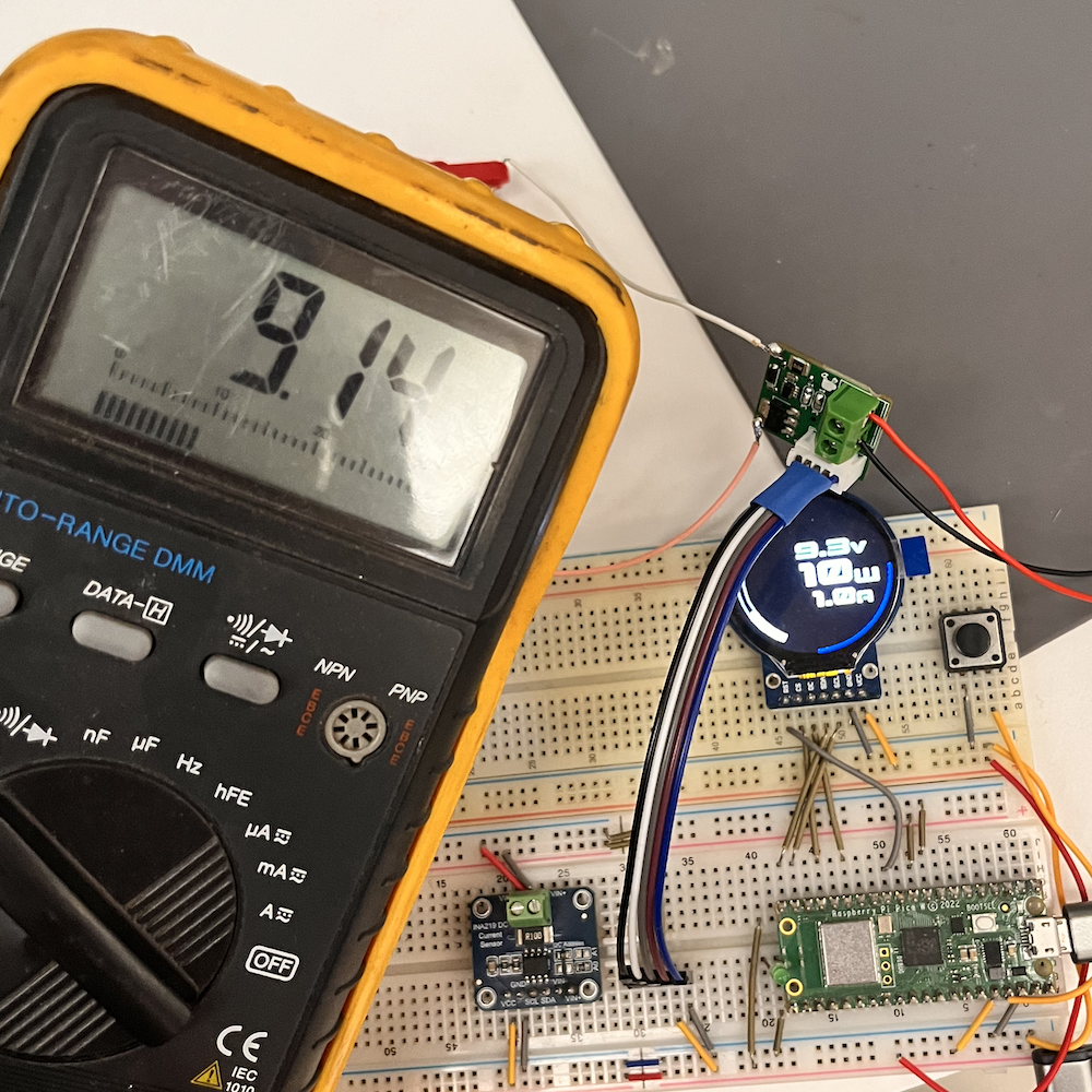
Next lets bridge some of these address select pads to check the address actually changes. In the image below I’ve connected SEL_0 to GND and SEL_1 to 3v3. This should set the address to 65 / 0b1000001 / 0x41.

Great that works too.
Next I hooked the output up to a 10 Ohm power resistor and ramped the input voltage to see how much voltage would be dropped over the MOSFET, seems fine! A touch test of the MOSFET also felt good even at 100W.
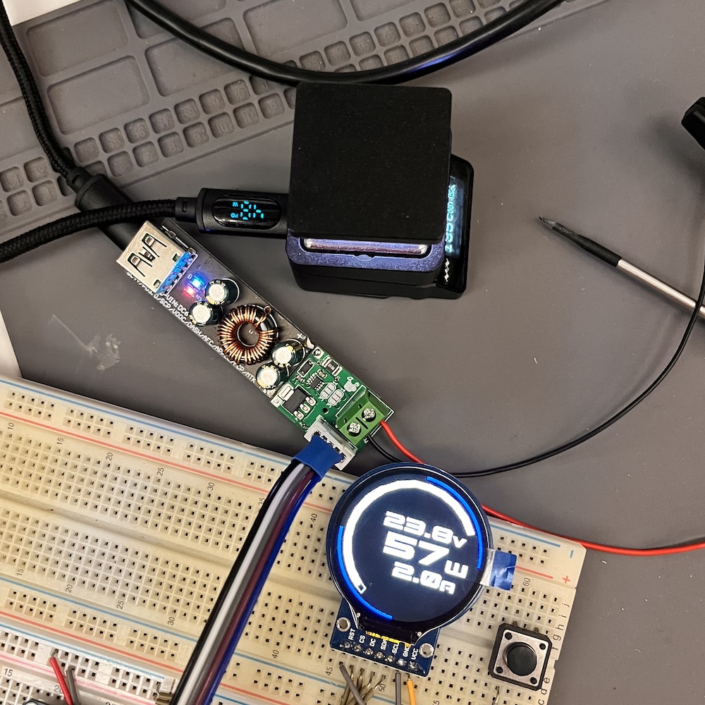
Finally I switched to the other board with the USB-C psu attached, ramped the supply to 24v and connected a hotplate as a test load. All seems good! Now I just need to get it all integrated into the case!
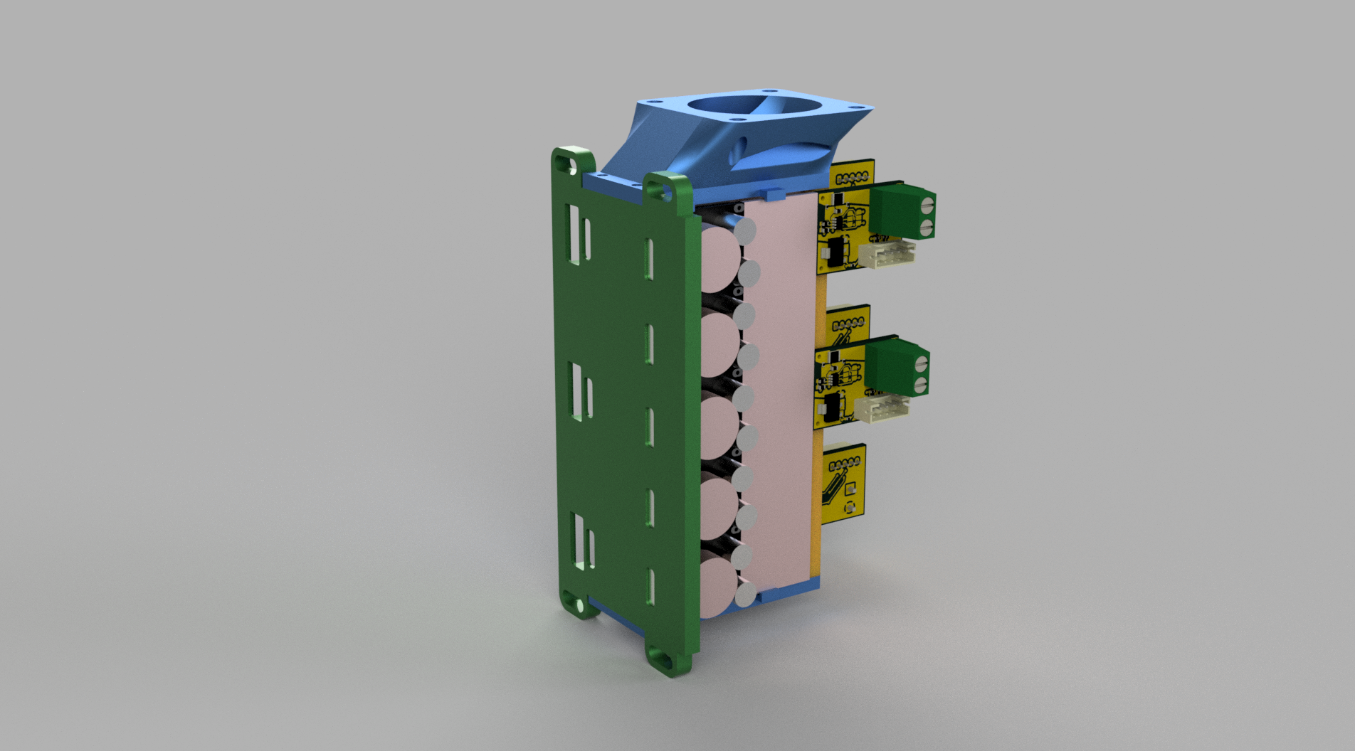
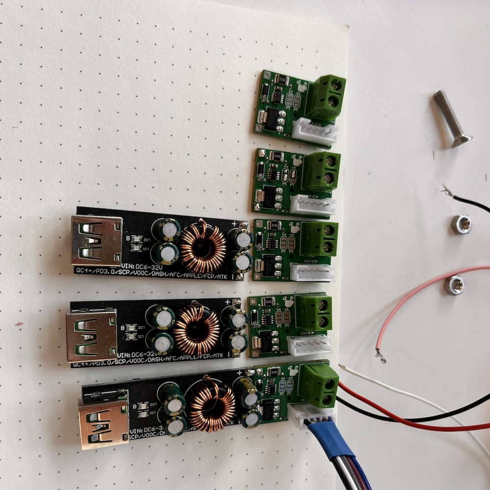
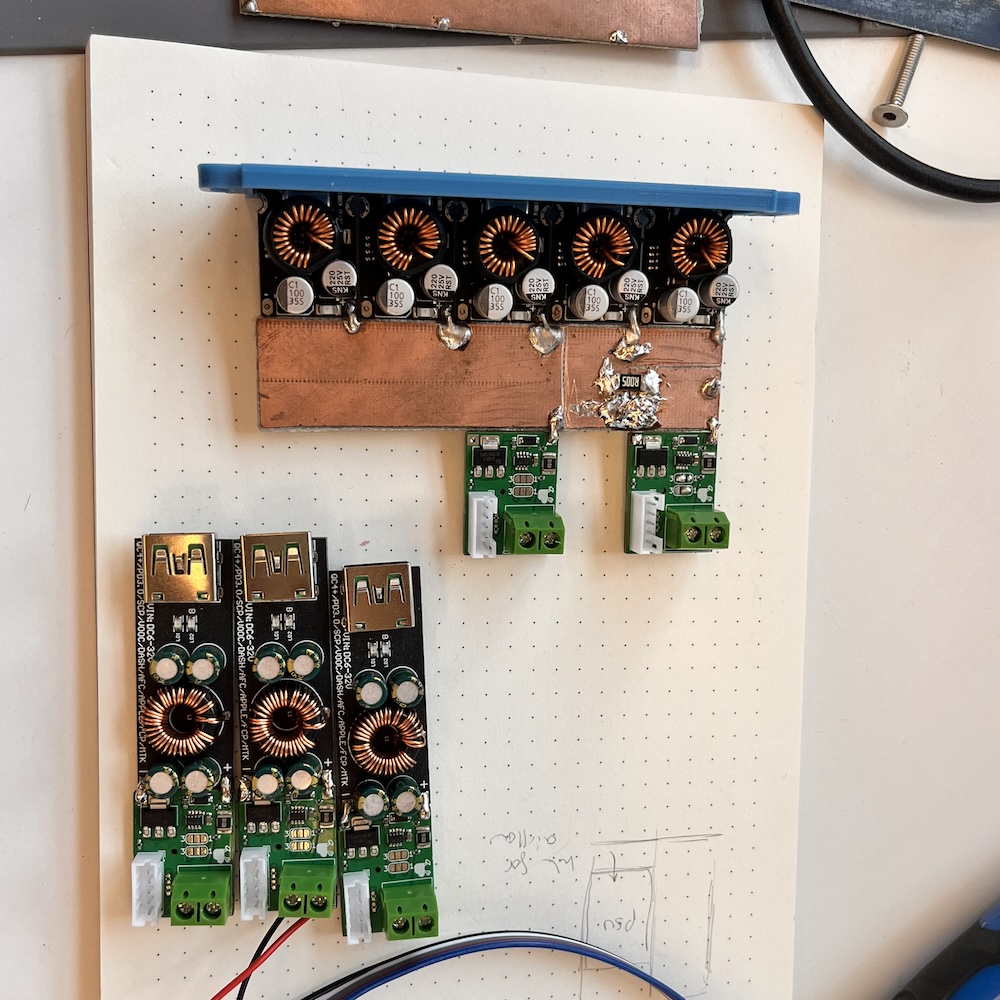
Next step was soldering up these modules, I’m going for 3 of the 100w modules and 5 of the 65w modules. I don’t want to order more of the custom PCBs so I’ve put the 65 modules in banks of 2 and 3 where each bank has a monitor pcb and then one for each of the 100W modules.
Ok bring up done!
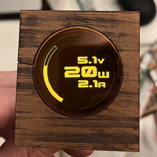
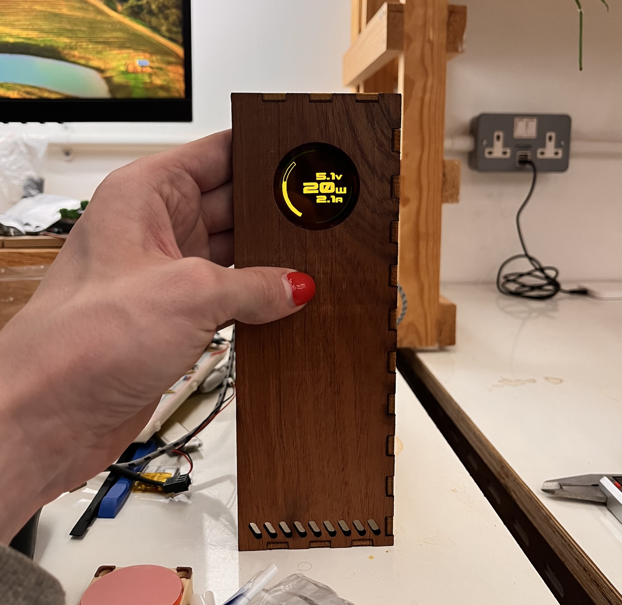
I updated the laser cut case design to 4mm ply instead of 3mm plywood. This made it feel much more solid in the hand. The 3mm version felt quick flimsy. I also cut out a circle of orange acrylic which I’m going to embed flush into the front panel. It gives the display this lovely warm orange cast that looks like some old VFD display. The front panel itself is a scrap bit of some hardwood from the workshop. I think it was an offcut from the table saw so it wasn’t uniformly 4mm throughout but the laser went through it happily and the thickness variation isn’t noticeable,
Next job is to finally finish the module that holds all the supply PCBs and mechanically couples them the rear panel and to a heatsink and fan.
Here’s a sneak peak of that in CAD, the pit at the top is a guide to draw air up through both the central heatsinks and a little bit over the top of each bank of PCBs.