I made my first PCB!
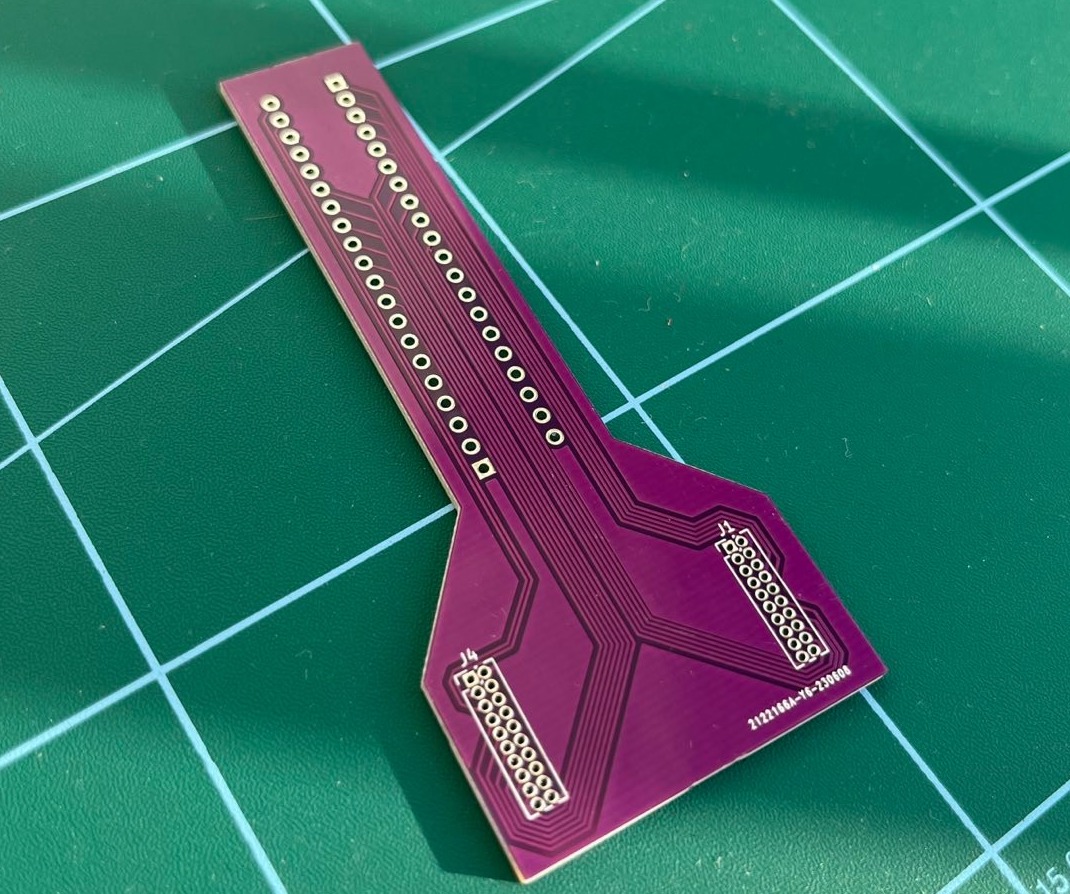
I’ve had a longstanding ambition to get a PCB manufactured but I’ve always put it off. Lately I had a need for a little adapter board to break out these 1.27mm spaced pins to 2.54mm pins that would fit into a breadboard. Feeling like it was a simple enough board I finally decided to fire up KiCad and give it a go.
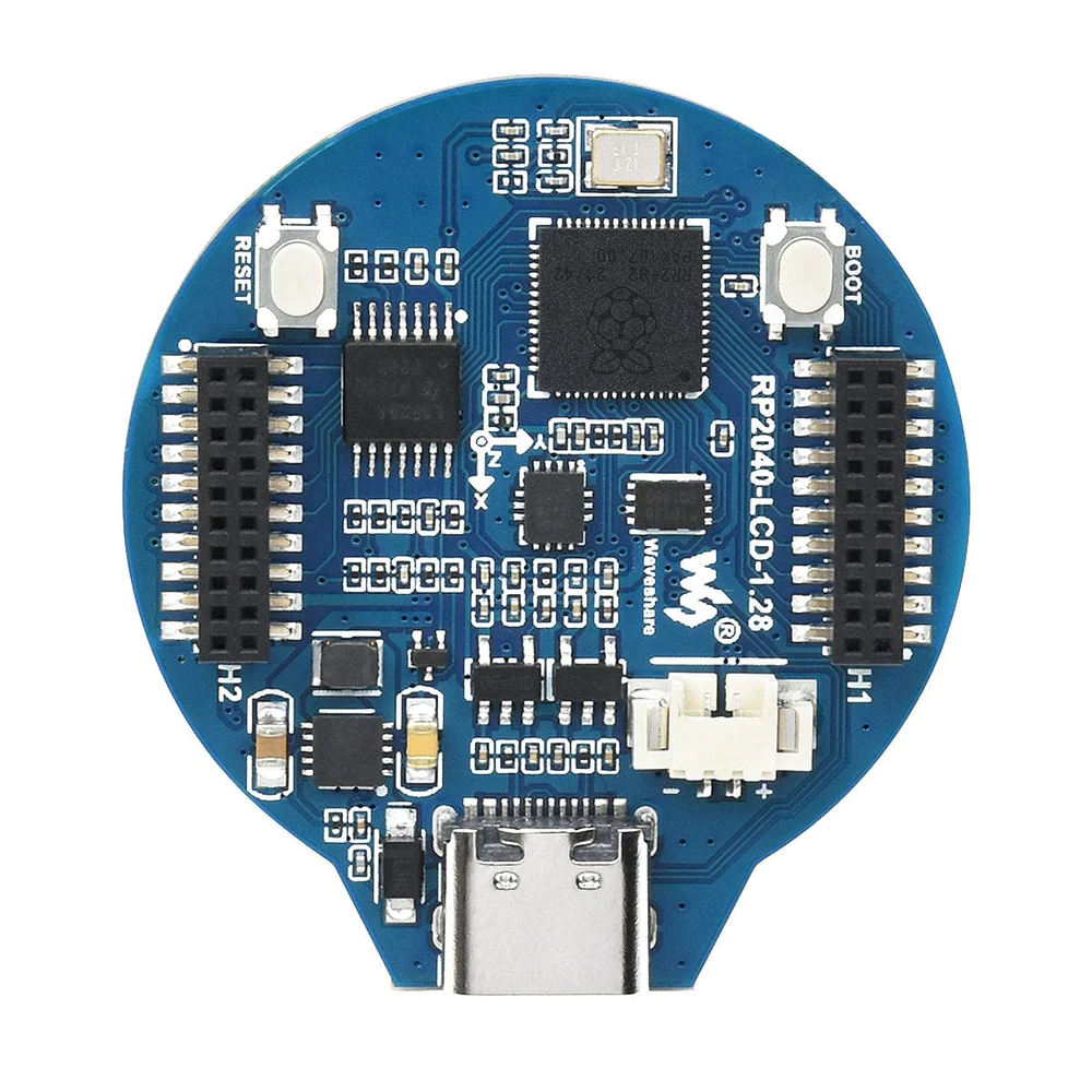
The 1.27mm headers in question are on the back of this cute round lcd breakout board.

So I fired up KiCAD and got to work, I had used it a couple time before but had never gotten as far as turning it into a real PCB. Well that changes today!
I used this excellent KiCAD plugin to generate the necessary gerber files that I could upload directly to JLPCB. Other fast cheap PCB manufactures exist, as you will know if you’ve ever watched an electronics themed youtube video. PCB manufacturers are to electronics YouTubers as mattresses peddlers are to podcasts.

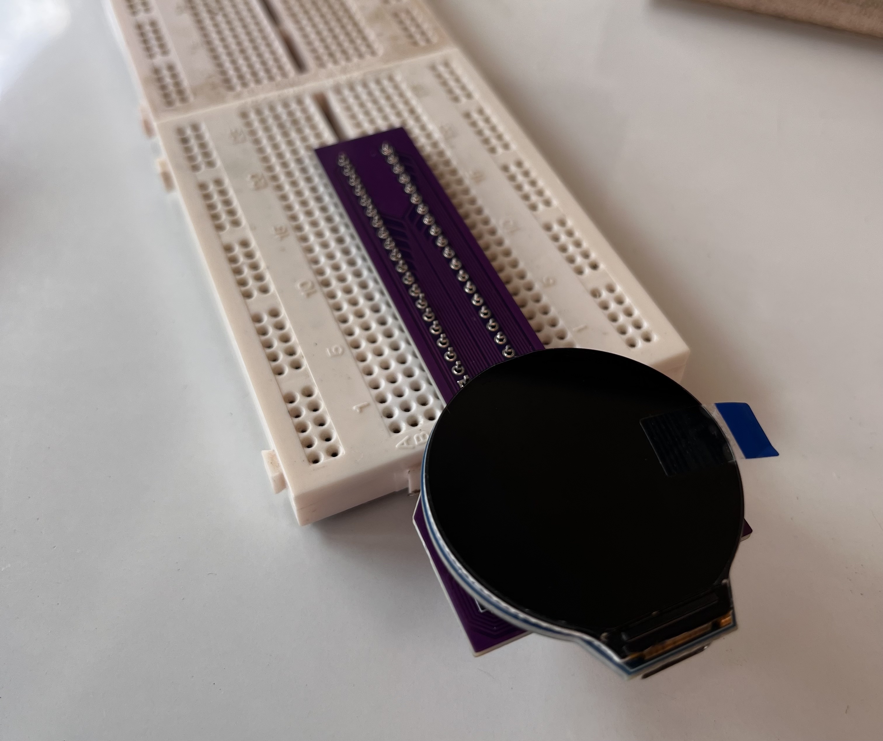
After getting the boards I soldering one up. Soldering the 1.27” header was surprisingly difficult to do without causing bridges. And those bridges were tough to remove once there. It didn’t help that I had run out off desoldering braid. Anyway I eventually got all the pins connected without overheating and delaminating the board.

Next I realised that I had made the obvious error: I put the 1.27” and 2.54” headers on the wrong sides from where the should go. The board isn’t reversible so that means the pin assignments are all wrong. By some miracle, the ground pins do have mirror symmetry so at least the ground plane is still the ground plane.
I had thought about trying to squeeze the pin assignments onto the silkscreen, thankfully I didn’t because this soldering mistake would have made those completely wrong.
I cloned the KiCAD file and swapped all the pin assignments around. Giving me this handy little cheat sheet.

Comments